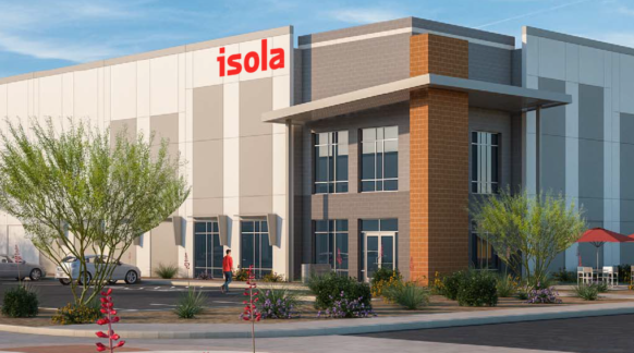
ISOLA ANNOUNCES NEW HEADQUARTERS LOCATION IN CHANDLER WITH 118,000 SQUARE FOOT LEASE
Chandler, Arizona, (August 27, 2019): Isola Group has completed a 118,000-square-foot lease to remain in Chandler and relocate its Corporate Offices, R&D and manufacturing operations. The company will be moving the Corporate Offices on October 7th, 2019 into…
Isola Shows PCB Materials for All Signals at Electronica 2022
Isola Group will be in Munich, Germany, for electronica 2022 with an assortment of circuit materials expected to meet or exceed the needs of the broad range of markets the international event serves. Set for November 15-18, 2022 in…
Isola Lays Foundations for Faster Circuits at DesignCon 2022
Isola Group will be exhibiting at the upcoming DesignCon 2022 expo and conference. The event, scheduled for April 5-7, 2022, at the Santa Clara Convention Center (Santa Clara, CA), provides…